
R & D process of optical transceiver
2017-08-25
As a global professional optical transceiver manufacturer, Fiberland get new and old customers consistent praise and trust rely on excellent R & D strength and professional quality service!
What raw materials are the optical modules made of? Generally speaking, there are three major parts:
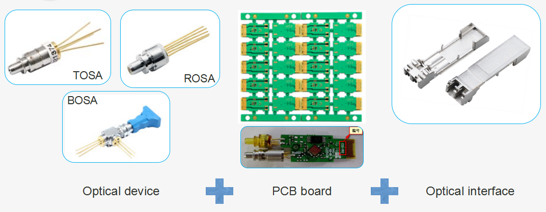
After understand the composition of the optical module, we will tell you about the development process of optical module.
Process:
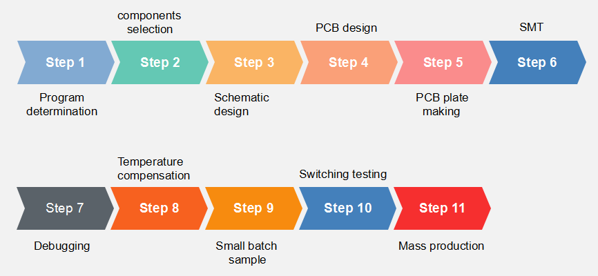
1. Program determination: Determine the framework and function of the module.
2. The selection of components: Including the optical components (TOSA, ROSA, BOSA) selection, IC selection and sample purchase.
3. Schematic design: Including MCU control circuit, module function power design and power circuit design.
4. PCB design: Including signal integrity design and high-speed circuit simulation, these work probably takes about half a month to a month.
5. PCB plate making: We need to provide PCB processing documents and Gerber documents to the plate factory for the production of PCB board.
6. SMT: Processing on the PCB is a complex process. The plate factory needs to provide the gerber file to the SMT factory, and we will provide the paste map / paste list to the SMT factory.
7. Optical module performance testing: Launch, receive testing and protocol functional debugging, also test pass luminosity, optical power, sensitivity, current, voltage and the eye, whether they are normal. It seems simple, but the whole process gathers the sweat and painstaking effort of the whole R & D team, each product is the crystallization of their wisdom.
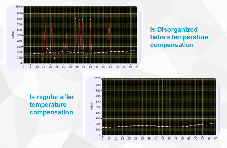
8. Temperature compensation: The technical engineer needs to spend a lot of time to do the temperature compensation.Increase or decrease every 5 degrees(or 10 degrees) as a node to calculate it’s slope.They need to write into to the corresponding IC(chip) of the optical transceiver after get the result.This work makes the technical engineer have to stay in front of the high and low temperature cycle aging box for a few hours or even longer.The increase in the raw material and the making cost,which is the cause of the high price of the industrial optical transceiver. The compared pictures of the working current before and after temperature compensation:
9. Small batch sample: It is necessary to pilot production in small quantities before mass production. If blindly put the product into the market in large quantities, once problems occur, it will lead to very serious consequences. After the sample is made, it is necessary to cooperate with the high and low temperature aging test (above 24 hours) to verify the stability and qualification rate of various parameters of the product.
10. Switching testing: Insert the module into the switch to check whether it works normally and audits the EEPROM information.
11. Mass production: After a variety of test and verification, by batch production.
For the entire R & D process, we are strict with each process. As a professional manufacturer, we focus on stable quality and quality services. We hope that our customers will get strong support from our cooperation!
XFP module,XFP transceiver,bidi sfp,SFP+ module,SFP+ transceiver Which is good? First choice Fiberland!Thanks for your concern, to learn more about Fiberland, please enter Fiberland website: http://www.fiberlandtec.com/
What raw materials are the optical modules made of? Generally speaking, there are three major parts:
After understand the composition of the optical module, we will tell you about the development process of optical module.
Process:
1. Program determination: Determine the framework and function of the module.
2. The selection of components: Including the optical components (TOSA, ROSA, BOSA) selection, IC selection and sample purchase.
3. Schematic design: Including MCU control circuit, module function power design and power circuit design.
4. PCB design: Including signal integrity design and high-speed circuit simulation, these work probably takes about half a month to a month.
5. PCB plate making: We need to provide PCB processing documents and Gerber documents to the plate factory for the production of PCB board.
6. SMT: Processing on the PCB is a complex process. The plate factory needs to provide the gerber file to the SMT factory, and we will provide the paste map / paste list to the SMT factory.
7. Optical module performance testing: Launch, receive testing and protocol functional debugging, also test pass luminosity, optical power, sensitivity, current, voltage and the eye, whether they are normal. It seems simple, but the whole process gathers the sweat and painstaking effort of the whole R & D team, each product is the crystallization of their wisdom.
8. Temperature compensation: The technical engineer needs to spend a lot of time to do the temperature compensation.Increase or decrease every 5 degrees(or 10 degrees) as a node to calculate it’s slope.They need to write into to the corresponding IC(chip) of the optical transceiver after get the result.This work makes the technical engineer have to stay in front of the high and low temperature cycle aging box for a few hours or even longer.The increase in the raw material and the making cost,which is the cause of the high price of the industrial optical transceiver. The compared pictures of the working current before and after temperature compensation:
9. Small batch sample: It is necessary to pilot production in small quantities before mass production. If blindly put the product into the market in large quantities, once problems occur, it will lead to very serious consequences. After the sample is made, it is necessary to cooperate with the high and low temperature aging test (above 24 hours) to verify the stability and qualification rate of various parameters of the product.
10. Switching testing: Insert the module into the switch to check whether it works normally and audits the EEPROM information.
11. Mass production: After a variety of test and verification, by batch production.
For the entire R & D process, we are strict with each process. As a professional manufacturer, we focus on stable quality and quality services. We hope that our customers will get strong support from our cooperation!
XFP module,XFP transceiver,bidi sfp,SFP+ module,SFP+ transceiver Which is good? First choice Fiberland!Thanks for your concern, to learn more about Fiberland, please enter Fiberland website: http://www.fiberlandtec.com/
RECENT BLOG POST
-
012019-10With the continuous development of 5G communication technology, 100G modules are gradually becoming popular. We know that there are many kinds of packages for 100G optical modules. From 2000 to now, the optical module package types have been rapidly developed. Its main package types are: GBIC, SFP, XENPAK, SNAP12, X2, XFP, SFP+, QSFP/QSFP+, CFP, CXP. In the fast-developing network era, some 100G optical modules avoid the risk of being eliminated, and upgraded and revised with the wave of the Internet, such as 100G CFP optical modules.
-
012019-101. What is the CWDM SFP? The CWDM optical module is an optical module using CWDM technology to implement the connection between the existing network device and the CWDM multiplexer/demultiplexer. When used with a CWDM multiplexer/demultiplexer, CWDM optical modules can increase network capacity by transmitting multiple data channels with separate optical wavelengths (1270 nm to 1610 nm) on the same single fiber.
-
012019-10AOC is the abbreviation of Active Optical Cables, which is called Active Optical Cables in Chinese. AOC active optical is to encapsulate two optical modules and cable together. Because the medium of transmission in the middle is optical cable, AOC optical module, which contains laser devices, has a higher price for DAC. However, its optical aperture is not exposed, it has high reliability, and its working distance can be customized for a long distance of less than 100 meters.
-
012019-10Dense Wavelength Division Multiplexing (DWDM) technology is capable of transmitting data in an optical fiber using bit wavelength parallel transmission or string line transmission using the wavelength of the laser.It is widely used in different fields of communication networks, including long-distance backbone networks, metropolitan area networks (MANs), residential access networks, and local area networks (LANs).The DWDM optical module is the optical module that uses this technology, so the DWDM optical module has high bandwidth and long-distance transmission characteristics.


